

What Is A 4-bit Shift Register Used For?
A shift register is a type of digital circuit using a cascade of flip-flops where the output of one flip-flop is connected to the input of the next. They share a unmarried clock indicate, which causes the information stored in the arrangement to shift from one location to the adjacent. By connecting the final flip-flop dorsum to the commencement, the data tin cycle inside the shifters for extended periods, and in this course they were used as a class of computer memory. In this role they are very like to the before delay-line memory systems and were widely used in the belatedly 1960s and early on 1970s to replace that form of retentivity.
In near cases, several parallel shift registers would be used to build a larger retentiveness pool known every bit a "bit array". Data was stored into the array and read back out in parallel, often equally a figurer discussion, while each bit was stored serially in the shift registers. There is an inherent trade-off in the pattern of bit arrays; putting more flip-flops in a row allows a unmarried shifter to shop more than bits, but requires more clock cycles to push the data through all of the shifters before the data can be read dorsum out over again.
Shift registers can have both parallel and serial inputs and outputs. These are frequently configured as "serial-in, parallel-out" (SIPO) or as "parallel-in, series-out" (PISO). There are also types that have both series and parallel input and types with serial and parallel output. There are besides "bidirectional" shift registers, which permit shifting in both directions: L& nbsp;→& nbsp;R or R& nbsp;→& nbsp;L. The series input and concluding output of a shift register can as well be connected to create a "round shift register". A PIPO register (parallel in, parallel out) is very fast – an output is given within a single clock pulse.
Serial-in serial-out (SISO) [edit]
Destructive readout [edit]
| Time | Output one | Output 2 | Output 3 | Output 4 |
|---|---|---|---|---|
| 0 | 0 | 0 | 0 | 0 |
| 1 | one | 0 | 0 | 0 |
| 2 | 0 | one | 0 | 0 |
| 3 | 1 | 0 | 1 | 0 |
| iv | 1 | one | 0 | i |
| 5 | 0 | 1 | 1 | 0 |
| 6 | 0 | 0 | 1 | 1 |
| 7 | 0 | 0 | 0 | 1 |
| viii | 0 | 0 | 0 | 0 |
These are the simplest kind of shift registers. The information cord is presented at "data in" and is shifted right 1 stage each time "information advance" is brought high. At each advance, the scrap on the far left (i.east. "data in") is shifted into the beginning flip-flop's output. The bit on the far right (i.e. "data out") is shifted out and lost.
The data is stored after each flip-flop on the "Q" output, then there are four storage "slots" bachelor in this arrangement, hence it is a 4-chip register. To give an thought of the shifting blueprint, imagine that the register holds 0000 (so all storage slots are empty). Equally "information in" presents one,0,1,1,0,0,0,0 (in that guild, with a pulse at "data accelerate" each time—this is called clocking or strobing) to the register, this is the event. The right paw cavalcade corresponds to the right-most flip-flop'southward output pin, and then on.
And so the serial output of the entire annals is 00010110. It tin exist seen that if data were to be connected to input, information technology would get exactly what was put in (10110000), only offset by iv "data advance" cycles. This organisation is the hardware equivalent of a queue. Also, at any time, the whole annals tin be ready to nil by bringing the reset (R) pins high.
This arrangement performs subversive readout – each datum is lost once information technology has been shifted out of the correct-almost bit.
Serial-in parallel-out (SIPO) [edit]

This configuration allows conversion from serial to parallel format. Data input is serial, as described in the SISO section in a higher place. Once the data has been clocked in, information technology may be either read off at each output simultaneously, or information technology can exist shifted out.
In this configuration, each flip-bomb is edge triggered. All flip-flops operate at the given clock frequency. Each input chip makes its way down to the Nth output afterward N clock cycles, leading to parallel output.
In cases where the parallel outputs should not change during the serial loading procedure, it is desirable to use a latched or buffered output. In a latched shift register (such as the 74595) the serial information is outset loaded into an internal buffer register, and then upon receipt of a load signal the state of the buffer register is copied into a set of output registers. In general, the practical application of the series-in/parallel-out shift annals is to convert information from serial format on a unmarried wire to parallel format on multiple wires.
Parallel-in serial-out (PISO) [edit]
This configuration has the data input on lines D1 through D4 in parallel format, D1 being the most significant bit. To write the data to the register, the Write/Shift control line must exist held LOW. To shift the data, the W/S command line is brought HIGH and the registers are clocked. The arrangement now acts every bit a PISO shift register, with D1 as the Data Input. Nonetheless, as long as the number of clock cycles is not more than than the length of the data-cord, the Data Output, Q, volition be the parallel information read off in social club.
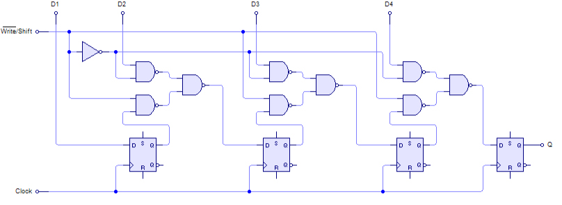
4-Fleck PISO Shift Register
The animation beneath shows the write/shift sequence, including the internal land of the shift register.

Uses [edit]

Toshiba TC4015BP – dual 4-stage static shift register (with serial input/parallel output)
One of the near mutual uses of a shift register is to convert between series and parallel interfaces. This is useful as many circuits piece of work on groups of bits in parallel, merely serial interfaces are simpler to construct. Shift registers tin can be used every bit unproblematic delay circuits. Several bidirectional shift registers could also be connected in parallel for a hardware implementation of a stack.
SIPO registers are commonly fastened to the output of microprocessors when more general-purpose input/output pins are required than are available. This allows several binary devices to be controlled using only two or 3 pins, but more slowly than by parallel output. The devices in question are attached to the parallel outputs of the shift register, and the desired state for all those devices can be sent out of the microprocessor using a single serial connection. Similarly, PISO configurations are commonly used to add more than binary inputs to a microprocessor than are available – each binary input (such as a push or more complicated circuitry) is fastened to a parallel input of the shift register, then the data is sent back via serial to the microprocessor using several fewer lines than originally required.
Shift registers can too be used as pulse extenders. Compared to monostable multivibrators, the timing has no dependency on component values, however, it requires external clock, and the timing accurateness is limited by a granularity of this clock. Example: Ronja Twister, where v 74164 shift registers create the cadre of the timing logic this way (schematic).
In early computers, shift registers were used to handle data processing: two numbers to be added were stored in two shift registers and clocked out into an arithmetics and logic unit (ALU) with the result beingness fed back to the input of one of the shift registers (the accumulator), which was one flake longer, since binary addition can but event in an answer that has the same size or is one scrap longer.
Many computer languages include instructions to "shift right" and "shift left" the data in a register, finer dividing by two or multiplying by two for each place shifted.
Very large series-in serial-out shift registers (thousands of bits in size) were used in a similar way to the earlier delay-line memory in some devices built in the early 1970s. Such memories were sometimes chosen "circulating memory". For example, the Datapoint 3300 final stored its brandish of 25 rows of 72 columns of half dozen-fleck upper-case characters using 54 (arranged in vi tracks of ix packs) 200-bit shift registers, providing storage for 1800 characters. The shift register design meant that scrolling the terminal display could be accomplished by just pausing the display output to skip ane line of characters.[1]
History [edit]
One of the get-go known examples of a shift register was in the Marker 2 Colossus, a lawmaking-breaking car congenital in 1944. It was a vi-stage device built of vacuum tubes and thyratrons.[2] A shift register was besides used in the IAS automobile, built by John von Neumann and others at the Institute for Advanced Study in the late 1940s.
Run across besides [edit]
- Delay-line memory
- Linear-feedback shift register (LFSR)
- Ring counter
- SerDes (Serializer/Deserializer)
- Serial Peripheral Interface Autobus
- Shift annals lookup table (SRL)
- Round buffer
References [edit]
- ^ bitsavers.org, DataPoint 3300 Maintenance Manual, December 1976.
- ^ Flowers, Thomas H. (1983), "The Pattern of Colossus", Annals of the History of Computing, 5 (3): 246, doi:ten.1109/MAHC.1983.10079

Source: https://en.wikipedia.org/wiki/Shift_register
Posted by: roccoloond1999.blogspot.com
0 Response to "What Is A 4-bit Shift Register Used For?"
Post a Comment